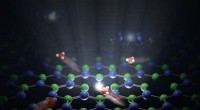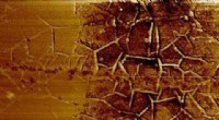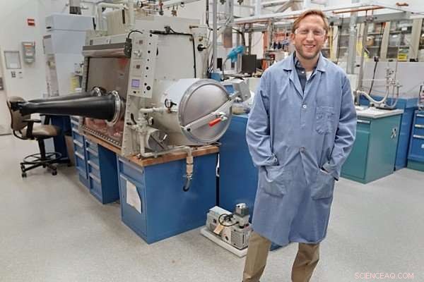
Le scientifique des matériaux Gregory Doerk dans le laboratoire de traitement des matériaux du CFN. Crédit :Laboratoire national de Brookhaven
Certains matériaux ont la capacité unique de s'auto-assembler en motifs et structures moléculaires organisés. Le scientifique des matériaux Gregory Doerk du groupe des nanomatériaux électroniques du Center for Functional Nanomaterials (CFN) - une installation utilisateur du bureau des sciences du département de l'Énergie des États-Unis (DOE) au Brookhaven National Laboratory - tire parti de cette capacité dans des matériaux appelés copolymères séquencés. En utilisant ces matériaux auto-assemblants, qui ont des chaînes de deux ou plusieurs molécules distinctes liées entre elles par des liaisons chimiques, Doerk dirige la formation de tels modèles et structures à l'échelle nanométrique. L'objectif ultime est de tirer parti de ces architectures nanométriques pour contrôler les propriétés des matériaux pour des applications telles que la conversion et le stockage de l'énergie solaire, catalyse, et optique.
L'auto-assemblage a récemment attiré beaucoup d'attention en tant qu'approche de nanofabrication. En quoi diffère-t-elle de l'approche traditionnellement utilisée ?
D'une manière générale, il existe deux plateformes pour la nanofabrication. Une plate-forme est la nanofabrication descendante, qui est l'approche traditionnelle utilisée pour fabriquer des puces informatiques et d'autres composants microélectroniques. La lumière est utilisée pour créer des motifs qui sont ensuite gravés dans des plaquettes de silicium. La technique de modelage utilisant la lumière est appelée lithographie optique. L'autre approche est la nanofabrication ascendante, ou l'auto-assemblage moléculaire. Les propriétés des matériaux sont codées dans leurs interactions faibles, qui poussent certains matériaux à se réunir et à former des configurations spécifiques, un peu comme des briques Lego, mais les briques se construisent toutes d'elles-mêmes pour former une structure.
La lithographie est généralement plus rapide et produit de manière plus fiable les structures conçues, mais nécessite des outils complexes. L'auto-assemblage est souvent plus lent et moins prédictif, mais il est peu coûteux et peut être plus facile. Il existe des façons de combiner les deux approches, et cette combinaison est connue sous le nom d'auto-assemblage dirigé. Les matériaux d'auto-assemblage tels que les films minces de copolymères séquencés sont commandés à l'aide de modèles modelés par lithographie standard. L'auto-assemblage dirigé améliore les processus de fabrication actuels, élargir le spectre des géométries de motifs possibles, et réduit le coût de la nanofabrication.
Vos recherches en auto-assemblage sont axées sur les copolymères à blocs. Qu'est-ce qui rend ces matériaux si spéciaux ?
Depuis les années 1950, les gens ont utilisé des copolymères triblocs (trois polymères réunis) dans des matériaux comme le caoutchouc synthétique. La plupart des polymères ne se mélangent pas. Essayer de mélanger des polymères, c'est un peu comme essayer de mélanger de l'huile et de l'eau.
Mais dans les copolymères à blocs, les chaînes polymères sont liées chimiquement les unes aux autres. Par exemple, les chaînes de copolymère dibloc (deux) sont reliées par une liaison covalente. Ce lien frustre leur volonté de « démixer ». Au lieu, si les copolymères séquencés reçoivent de l'énergie pour mobiliser leurs chaînes - par exemple en recuit (chauffage) le film de polymère sur une plaque chauffante au-dessus de sa température de transition vitreuse (quand un polymère passe d'un dur, matériau vitreux à un doux, caoutchouteux) - les chaînes se reconfigureront et s'assembleront en domaines à séparation de phases à l'échelle nanométrique. Ces domaines sont ordonnés en motifs à l'échelle nanométrique en fonction des caractéristiques inhérentes au copolymère séquencé. Par exemple, disons que nous avons deux polymères, A et B, réunis (copolymère dibloc). La longueur du bloc A par rapport à la longueur des deux blocs, la longueur totale des chaînes polymères, et les propriétés des polymères et la force de leur interaction (combien les polymères veulent se séparer) régissent la taille et la morphologie, ou forme, des structures résultantes. Si les chaînes sont trop courtes ou que leurs interactions répulsives sont trop faibles, les polymères vont se mélanger, provoquant l'état ordonné pour devenir un état désordonné et donc aucun motif ne se formera.
Au CFN, une grande partie de notre travail consiste à transférer les motifs et les structures réalisés par auto-assemblage, lithographie par faisceau d'électrons, ou la lithographie optique à notre installation de nanofabrication dans d'autres matériaux pour contrôler les propriétés des matériaux. Un bon exemple en est le travail du directeur du CFN, Chuck Black, utilisant des copolymères séquencés pour créer un motif auto-assemblé qui sert de modèle pour graver des cônes nanométriques sur des surfaces de silicium. Avec ces nanotextures, les surfaces de silicium transformées de miroirs réfléchissants en entièrement noires. C'est une façon d'utiliser des copolymères séquencés.
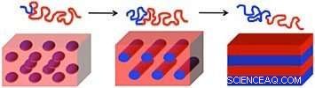
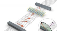
La longueur des blocs polymères (lignes ondulées rouges et bleues) et la force de leur interaction déterminent la forme des motifs résultants dans l'auto-assemblage du copolymère à blocs :(de gauche à droite) sphères, cylindres, et lamelles (feuilles). Crédit :Gregory Doerk
Mais nous voulons élargir la gamme de choses que nous pouvons faire avec l'auto-assemblage, et donc la gamme d'applications. Diversifier les motifs possibles avec l'auto-assemblage de copolymères à blocs est une grande partie de mes recherches.
Avez-vous pu élargir cette gamme ?
Une façon pour moi d'étendre ce que nous pouvons faire grâce à l'auto-assemblage est de créer des répliques inorganiques des structures auto-assemblées. Nous pouvons accomplir cette réplication grâce à un processus appelé synthèse par infiltration.
Par exemple, disons que vous avez un copolymère séquencé qui forme des lamelles (rayures) perpendiculaires à un substrat. Using an atomic-layer-deposition tool, it is possible to infiltrate those lamellae with a metal oxide and then remove the polymer, leaving behind metal oxide lines in a pattern determined by the polymer self-assembly. It is even possible to perform self-assembly and replica formation on top of previous replicas in an iterative way. What is really interesting is that the topography from the initial layer actually acts as a template dictating how polymer domains in the next layer line up. In the case of a second layer of lamellae perpendicular with the substrate, a self-assembled nanomesh is naturally created.
What other ways can you expand the range of self-assembled patterns?
One area in which I have collaborated with other members of the Electronic Nanomaterials Group is to study the blending of block copolymers that form lamellae with block copolymers that form cylinders. The really cool thing we learned is that you can precisely control which of these two patterns emerge in different areas of a substrate through an approach we call selective directed self-assembly. In a diblock copolymer, one of the blocks may be relatively more hydrophobic (water repelling) and the other may be relatively more hydrophilic (water attracting). So if a chemical pattern was made up of alternating hydrophobic and hydrophilic lines, the block copolymer molecules would self-assemble accordingly. By changing the spacing and width of the chemical line gratings (patterns) on the substrate, we were able to direct the self-assembling blocks into specific arrangements—either forming striped patterns (lamellae) or hexagonal dot arrays (cylinders). We can locally adjust the spacing and linewidth of the underlying chemical template to precisely control exactly where these line or dot patterns form on the same substrate, trop.
How big are the features of these self-assembled nanoscale patterns?
Block copolymers typically self-assemble into ordered periodic structures with a tunable repeat spacing between around 25 to 50 nanometers. Réellement, one of the projects I am currently working on is to increase the size range over which block copolymers form patterns. There is a lot of work in the scientific community to go to smaller and smaller sizes (approaching a few nanometers) for lithographic applications such as making computer chips. But for certain applications, you need larger sizes.
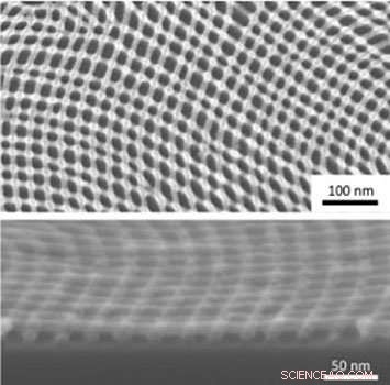
Plan view (top) and cross-sectional (bottom) scanning electron microscope images of an inorganic nanomesh created through iterative self-assembly and infiltration synthesis. Credit:Gregory Doerk
Par exemple, the wavelength range of visible light is about 400 (purple) to 700 (red) nanometers. Even 400 nanometers is still about 10 times larger than the approximately 40-nanometer length scale possible with most block copolymers. Par conséquent, light does not "see" the individual features of block copolymers.
Cependant, patterns with features closer to 200 nanometers in size can influence light in new ways, and I am working to scale block copolymer assembly to these sizes. One exciting application is using this approach to make "structural colors." Colors are typically made using dyes or pigments. Cependant, structural colors emerge from the way the light interacts with the nanomaterial—and so potentially one could make new types of lower-power displays through structural color.
Malheureusement, the process of forming patterns from block copolymers slows drastically, and even stops altogether, for these larger sizes. The development of self-assembled patterns is impeded by defective structures that form at the start of self-assembly. For these defects to "heal, " the block polymer must reconfigure, which involves pulling one chain through the domain of the other polymer, overcoming a large energy barrier to do so. As the size of the polymers increases, the energy barrier goes up exponentially—so exponentially slower healing!
Have you come up with any solutions to overcome this challenge?
My colleagues and I found that blending small-molecular-weight homopolymers (polymers made up of the same type of molecules) with the block copolymers makes it easier for the block copolymer chains to move around. Adding homopolymers promotes dramatic increases in the size of well-ordered pattern areas, ou "graines". Cependant, this addition alone does not let us form patterns with larger-size features from block copolymers. We also need to anneal the materials in a solvent vapor. Solvent vapor annealing involves putting a volatile solvent in the region of the diblock copolymer, causing the polymer film to swell. As the polymer film swells, the solvent molecules intersperse between polymer chains. This process has a plasticizing effect, making it easier for the polymer to move. So both mixing the block copolymer with a homopolymer and swelling it with a solvent are needed to speed the formation of large-scale patterns.
After annealing, we image the resulting patterns with scanning electron microscopes at CFN. We also perform x-ray scattering experiments at the Complex Materials Scattering beamline at Brookhaven Lab's National Synchrotron Light Source II [also a DOE Office of Science User Facility] to get a measure of the periodicity during the annealing process so we can determine how quickly the material self-assembles into an ordered pattern.
How do all of the different self-assembled patterns you generate translate to possible applications?
The work we do at CFN establishes the basis for producing new materials. Par exemple, consider the mesh pattern I described. My colleague Chang-Yong Nam and I are working on making a mesh of zinc oxide nanowires through infiltration synthesis of block copolymers. Zinc oxide is a versatile semiconducting material, and these nanowires have a lot of surface area, making them attractive for a number of applications—including photoelectrochemical water splitting (a way of converting sunlight into fuel by splitting water into hydrogen and oxygen). These semiconducting nanowires are also very responsive to environmental cues like light or chemicals. Given their large area uniformity, the meshes could be easily integrated into widely deployable gas sensors.
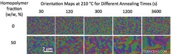
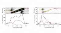
Without blending, the size of grains (single-color regions) of a diblock copolymer with a molecular weight of 36 kilograms/mole barely changes with thermal annealing over time (top row). Blending the block copolymer with homopolymers increases the grain size and speeds up the ordering process (bottom row). Credit:Gregory Doerk
How did you come to join CFN?
Après les études supérieures, I completed a postdoctoral appointment working at IBM in California. It was there that I learned about block copolymers, using them to make patterns for microelectronics. I did that for three years, and then in 2013 I joined a research group at HGST, a subsidiary of Western Digital that sells hard disk and solid-state drives. En premier, I worked on a project to create patterned nanoscale magnetic media onto which data is written to and read from, in order to enhance data density and stability.
Following that project, I moved into another area that was not very research oriented. At about this time, the current CFN Director, Chuck Black, gave a talk at HGST. Chuck's talk piqued my interest in CFN, and soon thereafter a position that very well fit my skills opened up. I applied, and joined CFN in 2015.
What was it like coming from industry to a national lab setting?
It definitely takes some getting used to. There is a lot less pressure in some ways but more pressure in other ways. Au CFN, you are expected to develop a lot more on your own as far as what direction you need to pursue on the basis of what is valuable to the lab. Dans l'industrie, the goals of the project are clear, and there are deliverables to keep you on the narrow path to achieving those goals. This is not to say that I did not do exploratory research for a portion of my time in industry.
The other difference at CFN is that I am more involved with the academic and industrial community at large. I have to manage my time so that I can perform my own research and help users with their research. I find it really cool that researchers from all over the world come to CFN. The talent and expertise of the staff are what make the CFN so great. The staff know backwards and forwards what they are doing in the areas they specialize in, and they are dedicated to helping others.
What are some of the ways you have helped users?
I regularly show users how to do block copolymer self-assembly and the etching process to transfer patterns into a substrate. Some users have employed these patterns as superhydrophobic textures to manipulate the flow of liquids in microfluidic devices, par exemple. Dans de nombreux cas, I help users develop a process when they need self-assembled patterns of varying sizes or shapes, to be applied to different substrates.
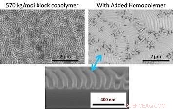
A comparison of scanning electron microscope images after solvent vapor annealing of a large block copolymer (top left) and the same copolymer with added homopolymer (top right) shows that the homopolymer can significantly improve pattern quality. The bottom image is a cross-sectional image of the top right sample. Credit:Gregory Doerk
I also help with the lithographic patterning of unusual materials. Par exemple, one user I am working with is trying to pattern protein hydrogels, looking at how they mechanically respond to swelling and de-swelling to understand how they might operate if injected into the body. Such protein hydrogels could have applications in biosensing, l'administration de médicaments, and wound healing.
Some users are interested in solvent vapor annealing, which is a very tricky process to control. So I am building a system with feedback control that can be set to maintain a solvent fraction of any given solvent. Autrement, if the amount of solvent varies over time, the self-assembly might not work at all (too little solvent) or result in a disordered state (too much solvent).
How did you become interested in research?
As an undergraduate at Case Western Reserve University, I majored in chemical engineering. One of my summer internships involved doing fuel cell work at a research lab. This internship led to another one at a fuel cell start-up, where I worked on sensors and solar cells. These internships gave me the opportunity to come up with ideas of my own and try different things. This exploration spurred me to pursue a doctoral degree at the University of California, Berkeley, where I continued my studies in chemical engineering.
I also think my undergraduate studies in philosophy, which I minored in, gave me a new understanding of the way science works. I really enjoyed reading about the philosophy of science, including books like Kuhn's The Structure of Scientific Revolutions. I learned how the views we often have are naïve or not accurate. There are lots of things people get wrong for a long time. But that does not mean they were not learning. Science is not perfect—but that is okay.
I was not the kid who grew up knowing he wanted to be a scientist. I liked philosophy and delving into critical thought. But I began to realize there is a lot of commonality between philosophy and science—in both fields, the aim is to gain knowledge about the world around us. But science is better because you can actually test things!